amphenol代理商
專業(yè)銷售Amphenol(安費(fèi)諾)全系列產(chǎn)品-英國2號(hào)倉庫
美國1號(hào)分類選型新加坡2號(hào)分類選型英國10號(hào)分類選型英國2號(hào)分類選型日本5號(hào)分類選型

在本站結(jié)果里搜索:    
熱門搜索詞:  Connectors  8910DPA43V02  Amphenol  UVZSeries 160VDC  70084122  IM21-14-CDTRI

NB3N121KMNG - 

3.3V 1:21 DIFF FANOUT CLOQFN 52 881MM PB FREE Code = 0457

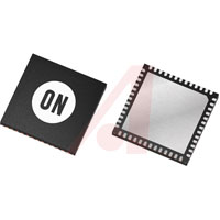
ON Semiconductor NB3N121KMNG
聲明:圖片僅供參考,請(qǐng)以實(shí)物為準(zhǔn)!
制造商產(chǎn)品編號(hào):
NB3N121KMNG
倉庫庫存編號(hào):
70400750
技術(shù)數(shù)據(jù)表:
View NB3N121KMNG Datasheet Datasheet
訂購熱線: 400-900-3095  0755-21000796, QQ:800152669, Email:sales@szcwdz.com
由于產(chǎn)品數(shù)據(jù)庫龐大,部分產(chǎn)品信息可能未能及時(shí)更新,下單前請(qǐng)與銷售人員確認(rèn)好實(shí)時(shí)在庫數(shù)量,謝謝合作!

NB3N121KMNG產(chǎn)品概述

The NB3N121K is a differential 1:21 Clock and Data fanout buffer with High-speed Current Steering Logic (HCSL) outputs optimized for ultra low propagation delay variation. The NB3N121K is designed with HCSL PCI Express clock distribution and FBDIMM applications in mind. Inputs can directly accept differential LVPECL, HCSL, and LVDS signals Single ended LVPECL, HCSL, LVCMOS, or LVTTL levels are accepted with a proper external Vth reference supply Input pins incorporate separate internal 50 Ω termination resistors allowing additional single ended system interconnect flexibility. Output drive current is set by connecting a 475 Ω resistor from IREF to GND. Outputs can also interface to LVDS receivers when terminated. The NB3N121K specifically guarantees low output–to–output skew. Optimal design, layout, and processing minimize skew within a device and from device to device. System designers can take advantage of the NB3N121K's performance to distribute low skew clocks across the backplane or the motherboard.

Features:
  • Typical Input Clock Frequency 100, 133, 166, 200, 266, 333 and 400 MHz
  • 340 ps Typical Rise and Fall Times
  • 800 ps Typical Propagation Delay
  • 100 ps Max Within Device Skew
  • 150 ps Max Device-to-Device Skew
  • tpd 100 ps Maximum Propagation Delay Variation Per Each Differential Pair
  • 0.1 ps Typical RMS Additive Phase Jitter
  • LVDS Output Levels Optional with Interface Termination
  • Operating Range: VCC = 3.0 V to 3.6 V with GND = 0 V
  • Typical HCSL Output Level (700 mV Peak-to-Peak)
  • These are Pb-Free Devices Applications
  • Clock Distribution
  • PCIe I, II, III
  • Networking
  • High End Computing
  • Routers

    End Products:
  • Servers
  • FBDIMM Memory Card
  • NB3N121KMNG產(chǎn)品信息

      Dimensions  8 x 8 x 0.95 mm  
      Height  0.037" (0.95mm)  
      Length  0.314" (8mm)  
      Logic Function  Clock Driver  
      Mounting Type  Surface Mount  
      Number of Clock Inputs  1  
      Number of Pins  52  
      Operating Voltage Range  3 to 3.6 V  
      Operation Mode  Differential, Single Ended  
      Package Type  QFN  
      Temperature, Operating, Maximum  +85 °C  
      Temperature, Operating, Minimum  -40 °C  
      Temperature, Operating, Range  -40 to +85 °C  
      Width  0.315" (8mm)  
    關(guān)鍵詞         

    NB3N121KMNG相關(guān)搜索

    Dimensions 8 x 8 x 0.95 mm  ON Semiconductor Dimensions 8 x 8 x 0.95 mm  Clock Drivers Dimensions 8 x 8 x 0.95 mm  ON Semiconductor Clock Drivers Dimensions 8 x 8 x 0.95 mm   Height 0.037" (0.95mm)  ON Semiconductor Height 0.037" (0.95mm)  Clock Drivers Height 0.037" (0.95mm)  ON Semiconductor Clock Drivers Height 0.037" (0.95mm)   Length 0.314" (8mm)  ON Semiconductor Length 0.314" (8mm)  Clock Drivers Length 0.314" (8mm)  ON Semiconductor Clock Drivers Length 0.314" (8mm)   Logic Function Clock Driver  ON Semiconductor Logic Function Clock Driver  Clock Drivers Logic Function Clock Driver  ON Semiconductor Clock Drivers Logic Function Clock Driver   Mounting Type Surface Mount  ON Semiconductor Mounting Type Surface Mount  Clock Drivers Mounting Type Surface Mount  ON Semiconductor Clock Drivers Mounting Type Surface Mount   Number of Clock Inputs 1  ON Semiconductor Number of Clock Inputs 1  Clock Drivers Number of Clock Inputs 1  ON Semiconductor Clock Drivers Number of Clock Inputs 1   Number of Pins 52  ON Semiconductor Number of Pins 52  Clock Drivers Number of Pins 52  ON Semiconductor Clock Drivers Number of Pins 52   Operating Voltage Range 3 to 3.6 V  ON Semiconductor Operating Voltage Range 3 to 3.6 V  Clock Drivers Operating Voltage Range 3 to 3.6 V  ON Semiconductor Clock Drivers Operating Voltage Range 3 to 3.6 V   Operation Mode Differential, Single Ended  ON Semiconductor Operation Mode Differential, Single Ended  Clock Drivers Operation Mode Differential, Single Ended  ON Semiconductor Clock Drivers Operation Mode Differential, Single Ended   Package Type QFN  ON Semiconductor Package Type QFN  Clock Drivers Package Type QFN  ON Semiconductor Clock Drivers Package Type QFN   Temperature, Operating, Maximum +85 °C  ON Semiconductor Temperature, Operating, Maximum +85 °C  Clock Drivers Temperature, Operating, Maximum +85 °C  ON Semiconductor Clock Drivers Temperature, Operating, Maximum +85 °C   Temperature, Operating, Minimum -40 °C  ON Semiconductor Temperature, Operating, Minimum -40 °C  Clock Drivers Temperature, Operating, Minimum -40 °C  ON Semiconductor Clock Drivers Temperature, Operating, Minimum -40 °C   Temperature, Operating, Range -40 to +85 °C  ON Semiconductor Temperature, Operating, Range -40 to +85 °C  Clock Drivers Temperature, Operating, Range -40 to +85 °C  ON Semiconductor Clock Drivers Temperature, Operating, Range -40 to +85 °C   Width 0.315" (8mm)  ON Semiconductor Width 0.315" (8mm)  Clock Drivers Width 0.315" (8mm)  ON Semiconductor Clock Drivers Width 0.315" (8mm)  
    電話:400-900-3095
    QQ:800152669
    關(guān)于我們 | Amphenol簡介 | Amphenol產(chǎn)品 | Amphenol產(chǎn)品應(yīng)用 | Amphenol動(dòng)態(tài) | 按系列選型 | 按產(chǎn)品規(guī)格選型 | Amphenol選型手冊(cè) | 付款方式 | 聯(lián)系我們
    Copyright © 2017 habitrun.com All Rights Reserved. 技術(shù)支持:電子元器件 ICP備案證書號(hào):粵ICP備11103613號(hào)